


Lattice MachXO 非挥发PLD开发方案
2010/3/25 9:31:00
Lattice 公司的MachXO系列是非挥发可无限次编程的可编程逻辑器件(PLD),LUT从256到2280. MachXO把CPLD和FPGA的特性集中在单个芯片上:胶合逻辑,总线桥,总线接口,上电控制和控制逻辑等. MachXO系列设计用于各种低密度的应用如消费类电子,汽车电子,通信,计算,工业和医疗.本文介绍了MachXO系列的主要特性和优势,以及MachXO系列PLD开发套件主要特性, 评估板方框图和详细电路图和所用元件清单.
The MachXO is optimized to meet the requirements of applications traditionally addressed by CPLDs and low capacity FPGAs: glue logic, bus bridging, bus interfacing, power-up control, and control logic. These devices bring together the best features of CPLD and FPGA devices on a single chip.
The MachXO family of non-volatile infinitely reconfigurable Programmable Logic Devices (PLDs) is designed for applications traditionally implemented using CPLDs or low-capacity FPGAs. Widely adopted in a broad range of applications that require general purpose I/O expansion, interface bridging and power-up management functions, MachXO PLDs offer the benefits of increased system integration by providing embedded memory, built-in PLLs, high performance LVDS I/O, remote field upgrade (TransFRTM technology) and a low power sleep mode, all in a single-device.
Designed for a broad range of low density applications, the MachXO PLD family is used in a variety of end markets including consumer, automotive, communications, computing, industrial and medical.
MachXO主要优势:
Powers up in less than 1ms enabling precise control during system boot-up
No external configuration memory required reducing total system cost
Efficient cost effective data buffering
Integrated clock management reducing total system cost
Interface with multiple voltages and speed critical functions
Reduces standby power to <100uA
Allows remote field upgrades while the equipment operates
MachXO主要特性:
Non-volatile, Infinitely Reconfigurable
Instant-on–powers up in microseconds
Single chip, no external configuration memory required
Excellent design security, no bit stream to intercept
Reconfigure SRAM based logic in milliseconds
SRAM and non-volatile memory programmable through JTAG port
Supports background programming of non-volatile memory
Sleep Mode
Allows up to 100x static current reduction
TransFR Reconfiguration (TFR)
In-field logic up date while system operates
High I/O to Logic Density
256 to 2280 LUT4s
73 to 271 I/Os with extensive package options
Density migration supported
Lead free/RoHS compliant packaging
Embedded and Distributed Memory
Up to 27.6 Kbits sysMEM Embedded Block RAM
Up to 7.5 Kbits distributed RAM
Dedicated FIFO control logic
Flexible I/O Buffer
Programmable sysIO buffer supports wide range of interfaces:
LVCMOS 3.3/2.5/1.8/1.5/1.2
LVTTL
PCI
LVDS, Bus-LVDS, LVPECL, RSDS
sysCLOCK PLLs
Up to two analog PLLs per device
Clock multiply, divide, and phase shifting
System Level Support
IEEE Standard 1149.1 Boundary Scan
Onboard oscillator
Devices operate with 3.3V, 2.5V, 1.8V or 1.2V power supply
IEEE 1532 compliant in-system programming
MachXO Family Selection Guide

The MachXO Mini Development Kit is an easy to use, low-cost platform to accelerate the evaluation of MachXO PLDs. The kit features the MachXO LCMXO2280 device, 2 Mbit SPI Flash and 1 Mbit SRAM memory, a temperature sensor, an expansion header for I2C and SPI interfaces, and several LEDs and user switches.
Using the preloaded mini system-on-chip (Mini SoC) design provided with the development kit, you can now test within minutes I2C, SPI, UART and SRAM interfaces in addition to the 8-bit LatticeMico8 microcontroller. You can then build your own designs using the free downloadable reference design source code, implementing these features in less than an hour. The board also features USB channels for JTAG programming and debugging from a host PC. A pin header provides access to a variety of PIO banks of the MachXO PLD and the on-board I2C bus. The board can be controlled with menu driven interface via terminal programs running on a host PC.
MachXO PLD开发套件包括:
MachXO Mini Evaluation Board
The MachXO Mini Evaluation Board features the following:
MachXO PLD: LCMXO2280C-4TN144C
2 Mbit SPI Flash Memory
1 Mbit SRAM
I2C Temperature Sensor
USB mini jack sockets for power, JTAG programming, and RS-232 debugging
2X16 header for off-board expansion provides access to top and right side MachXO banks
Push buttons for sleep mode and reset
4-bit DIP switch to user-defined inputs
ADC/DAC circuit
Sleep circuit
8 LEDs for user-defined outputs
RoHS-compliant packaging and process
Two USB connector cables
QuickSTART Guide

图1.MachXO Mini 评估板外形图

图2.Mini SoC 方框图

图3.MachXO Mini 评估板方框图

图4.MachXO Mini 评估板电路图(1)

图5.MachXO Mini 评估板电路图(2)

图6.MachXO Mini 评估板电路图(3)

图7.MachXO Mini 评估板电路图(4)

图8.MachXO Mini 评估板电路图(5)

图9.MachXO Mini 评估板电路图(6)

图10.MachXO Mini 评估板电路图(7)
材料清单(BOM):


The MachXO is optimized to meet the requirements of applications traditionally addressed by CPLDs and low capacity FPGAs: glue logic, bus bridging, bus interfacing, power-up control, and control logic. These devices bring together the best features of CPLD and FPGA devices on a single chip.
The MachXO family of non-volatile infinitely reconfigurable Programmable Logic Devices (PLDs) is designed for applications traditionally implemented using CPLDs or low-capacity FPGAs. Widely adopted in a broad range of applications that require general purpose I/O expansion, interface bridging and power-up management functions, MachXO PLDs offer the benefits of increased system integration by providing embedded memory, built-in PLLs, high performance LVDS I/O, remote field upgrade (TransFRTM technology) and a low power sleep mode, all in a single-device.
Designed for a broad range of low density applications, the MachXO PLD family is used in a variety of end markets including consumer, automotive, communications, computing, industrial and medical.
MachXO主要优势:
Powers up in less than 1ms enabling precise control during system boot-up
No external configuration memory required reducing total system cost
Efficient cost effective data buffering
Integrated clock management reducing total system cost
Interface with multiple voltages and speed critical functions
Reduces standby power to <100uA
Allows remote field upgrades while the equipment operates
MachXO主要特性:
Non-volatile, Infinitely Reconfigurable
Instant-on–powers up in microseconds
Single chip, no external configuration memory required
Excellent design security, no bit stream to intercept
Reconfigure SRAM based logic in milliseconds
SRAM and non-volatile memory programmable through JTAG port
Supports background programming of non-volatile memory
Sleep Mode
Allows up to 100x static current reduction
TransFR Reconfiguration (TFR)
In-field logic up date while system operates
High I/O to Logic Density
256 to 2280 LUT4s
73 to 271 I/Os with extensive package options
Density migration supported
Lead free/RoHS compliant packaging
Embedded and Distributed Memory
Up to 27.6 Kbits sysMEM Embedded Block RAM
Up to 7.5 Kbits distributed RAM
Dedicated FIFO control logic
Flexible I/O Buffer
Programmable sysIO buffer supports wide range of interfaces:
LVCMOS 3.3/2.5/1.8/1.5/1.2
LVTTL
PCI
LVDS, Bus-LVDS, LVPECL, RSDS
sysCLOCK PLLs
Up to two analog PLLs per device
Clock multiply, divide, and phase shifting
System Level Support
IEEE Standard 1149.1 Boundary Scan
Onboard oscillator
Devices operate with 3.3V, 2.5V, 1.8V or 1.2V power supply
IEEE 1532 compliant in-system programming
MachXO Family Selection Guide
The MachXO Mini Development Kit is an easy to use, low-cost platform to accelerate the evaluation of MachXO PLDs. The kit features the MachXO LCMXO2280 device, 2 Mbit SPI Flash and 1 Mbit SRAM memory, a temperature sensor, an expansion header for I2C and SPI interfaces, and several LEDs and user switches.
Using the preloaded mini system-on-chip (Mini SoC) design provided with the development kit, you can now test within minutes I2C, SPI, UART and SRAM interfaces in addition to the 8-bit LatticeMico8 microcontroller. You can then build your own designs using the free downloadable reference design source code, implementing these features in less than an hour. The board also features USB channels for JTAG programming and debugging from a host PC. A pin header provides access to a variety of PIO banks of the MachXO PLD and the on-board I2C bus. The board can be controlled with menu driven interface via terminal programs running on a host PC.
MachXO PLD开发套件包括:
MachXO Mini Evaluation Board
The MachXO Mini Evaluation Board features the following:
MachXO PLD: LCMXO2280C-4TN144C
2 Mbit SPI Flash Memory
1 Mbit SRAM
I2C Temperature Sensor
USB mini jack sockets for power, JTAG programming, and RS-232 debugging
2X16 header for off-board expansion provides access to top and right side MachXO banks
Push buttons for sleep mode and reset
4-bit DIP switch to user-defined inputs
ADC/DAC circuit
Sleep circuit
8 LEDs for user-defined outputs
RoHS-compliant packaging and process
Two USB connector cables
QuickSTART Guide
图1.MachXO Mini 评估板外形图
图2.Mini SoC 方框图
图3.MachXO Mini 评估板方框图
图4.MachXO Mini 评估板电路图(1)
图5.MachXO Mini 评估板电路图(2)
图6.MachXO Mini 评估板电路图(3)
图7.MachXO Mini 评估板电路图(4)
图8.MachXO Mini 评估板电路图(5)
图9.MachXO Mini 评估板电路图(6)
图10.MachXO Mini 评估板电路图(7)
材料清单(BOM):


 投诉建议
投诉建议
提交
查看更多评论
其他资讯

助力企业恢复“战斗状态”:MyMRO我的万物集·固安捷升级开工场景方案
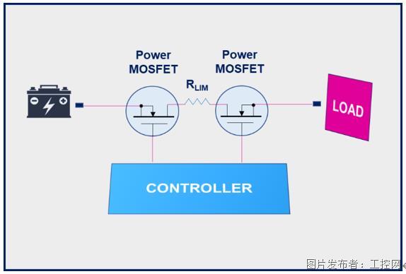
车规MOSFET技术确保功率开关管的可靠性和强电流处理能力

未来十年, 化工企业应如何提高资源效率及减少运营中的碳足迹?
2023年制造业“开门红”,抢滩大湾区市场锁定DMP工博会

2023钢铁展洽会4月全新起航 将在日照触发更多商机